

















 Back to List
Ask HJT | How Thin Can HJT Wafers Go—Without Compromising Performance?


Silicon wafers are one of the largest material cost components in solar cell manufacturing and a major contributor to the carbon footprint of photovoltaic products. As the PV industry moves toward thinner wafers, one question becomes increasingly important: how can manufacturers reduce silicon consumption without compromising efficiency, production yield, or long-term reliability?
In this episode of Dinto Solar’s Ask HJT, we explore why wafer quality matters for high-efficiency HJT cells, what enables HJT to process ultrathin wafers, and how 110 μm wafer technology translates into tangible customer value.
Q1: Why is wafer quality especially important for high-efficiency HJT cells?
A. HJT wafers must be produced using the float-zone method to reduce oxygen content.
B. HJT’s excellent surface passivation makes bulk carrier lifetime and wafer quality critical to achieving high voltage and efficiency.
C. HJT requires much heavier boron doping than other solar cell technologies.
D. HJT wafers must be polished on both sides before amorphous silicon films can be deposited.
Wafer Quality Matters
HJT cells use thin amorphous silicon layers to form carrier-selective, passivating contacts on crystalline silicon. These layers strongly suppress surface recombination, allowing more photogenerated carriers to be collected.
As surface losses are reduced, the crystalline silicon wafer’s bulk quality—including minority-carrier lifetime and defect density—becomes increasingly important to achieving high open-circuit voltage and conversion efficiency.
High-quality n-type monocrystalline silicon wafers are therefore particularly well suited to HJT. They can provide long minority-carrier lifetimes and are not susceptible to the conventional boron–oxygen-related light-induced degradation found in boron-doped p-type wafers. Meanwhile, HJT’s intrinsic amorphous silicon layers provide excellent surface passivation, further reducing carrier recombination losses.
✅ Correct answer to Q1: B
Q2: Which technical features enable HJT to handle ultrathin wafers? (Multiple answers)
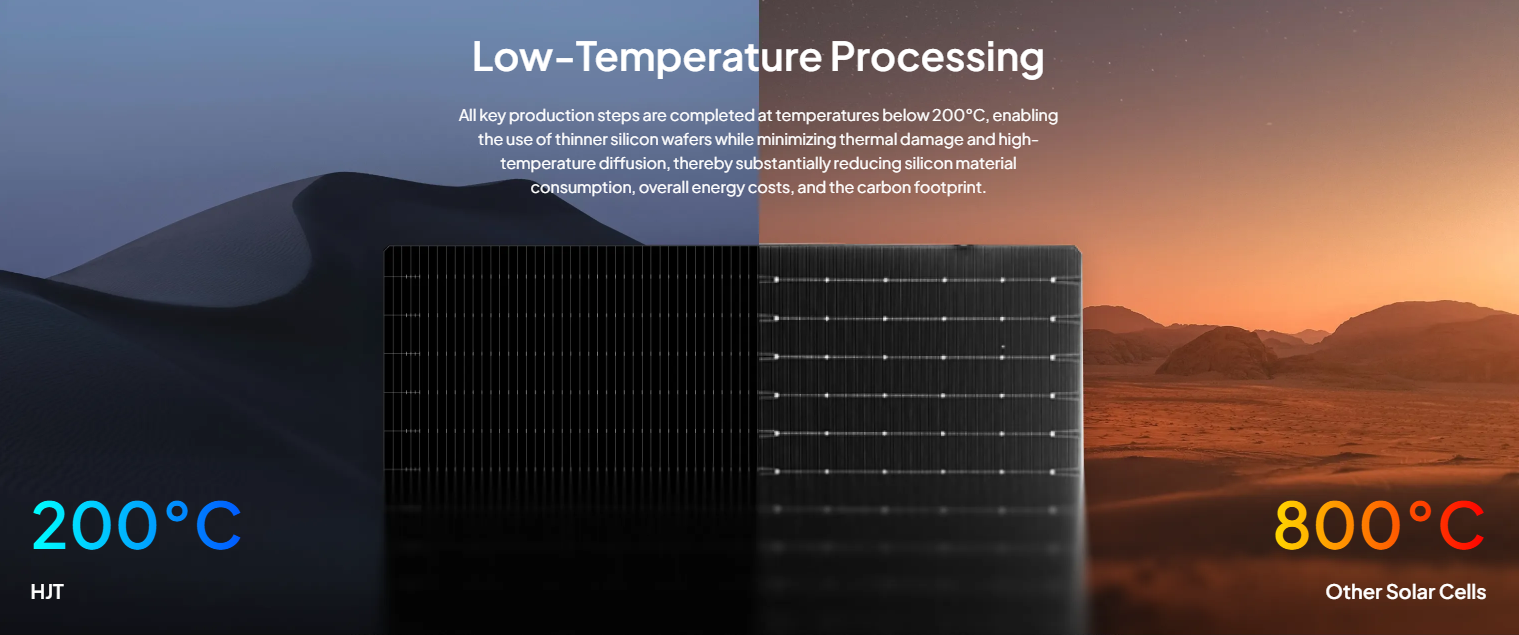
A. A low-temperature process, typically below approximately 200°C, reduces thermal stress on thin wafers.
B. A near-symmetrical double-sided cell structure helps balance film-induced stress and reduce wafer bowing.
C. HJT-specific wafers are inherently harder than TOPCon and BC wafers, making them less prone to breakage.
D. An additional physical reinforcement film is applied before the cells leave the factory.
Dual Protection
HJT combines two important process advantages that support the use of ultrathin wafers.
Low-temperature processing
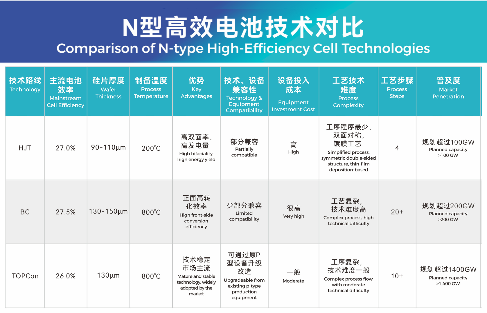
Key HJT processes—including amorphous silicon deposition, TCO deposition, and metallization—are performed at relatively low temperatures, typically below approximately 200°C.
Avoiding high-temperature diffusion reduces thermal expansion and contraction stress, helping lower the risk of wafer deformation, microcracks, and breakage during production.
Near-symmetrical double-sided processing
HJT cells use thin-film stacks on both sides of the crystalline silicon wafer. Although the functional layers on the two sides are not completely identical, the near-symmetrical double-sided structure helps balance film-induced mechanical stress.
This improves dimensional stability during manufacturing and reduces the risk of bowing and breakage as wafers become thinner.
✅ Correct answers to Q2: A, B
Q3: What practical value does Dinto Solar create for customers by adopting 110 μm HJT wafers? (Multiple answers)
A. Lower silicon consumption and cell manufacturing costs.
B. A lower product carbon footprint that supports low-carbon procurement requirements.
C. Greater material efficiency and lower exposure to silicon-related supply-chain costs.
D. Double the cell efficiency.
Value Through Thinning
Lower silicon consumption and manufacturing costs
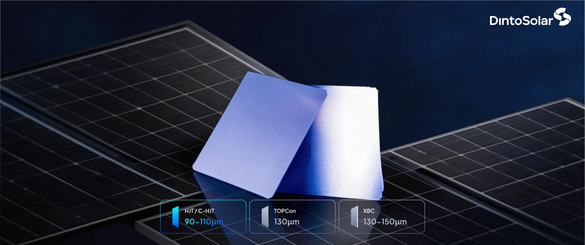
Reducing wafer thickness from 130 μm to 110 μm and below allows more wafers to be produced from the same amount of silicon.
Lower silicon consumption per wafer improves material utilization and can reduce cell manufacturing costs, although the final cost benefit also depends on slicing losses, production yield, and overall process efficiency.
A lower product carbon footprint
Polysilicon production and wafer manufacturing are among the most energy- and carbon-intensive stages of the crystalline silicon PV value chain. Thinner wafers require less silicon per watt, helping reduce the embodied carbon footprint of solar products.
As global markets place greater emphasis on product carbon footprints, supply-chain transparency, and low-carbon procurement, reduced silicon consumption can strengthen the environmental competitiveness of PV modules.
Greater resource efficiency
Using less silicon for each cell improves resource efficiency and reduces exposure to fluctuations in silicon-related material costs and supply conditions.
For project owners and customers, this supports a more efficient and resilient PV supply chain while contributing to lower lifecycle costs.
✅ Correct answers to Q3: A, B, C
In the photovoltaic industry’s ongoing pursuit of lower costs and higher efficiency, wafer thickness cannot be considered independently from wafer quality, manufacturing yield, and cell architecture.
HJT’s excellent surface passivation places a premium on high-quality crystalline silicon with long minority-carrier lifetime. At the same time, its low-temperature manufacturing process and near-symmetrical double-sided structure help reduce the thermal and mechanical stresses associated with processing thinner wafers.
Leveraging these advantages, Dinto Solar has already adopted 110 μm ultrathin wafers at scale in its HJT production lines and has developed the technical capability to advance toward wafer thicknesses below 100 μm.
The value of ultrathin-wafer technology extends beyond simply using less silicon. By combining material efficiency, a lower product carbon footprint, strong manufacturing compatibility, and reliable cell performance, Dinto Solar’s HJT technology helps customers achieve lower LCOE and stronger project returns throughout the full system lifecycle.
We welcome you to share your own insights on heterojunction technology or let us know which HJT questions you would like us to explore next. Selected topics will be featured in future installments of Ask HJT.