


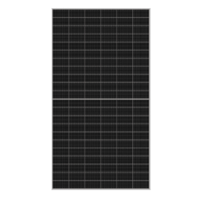


WHAT IS HJT TECHNOLOGY?
Intrinsic thin-film heterojunction (HJT) cells feature a symmetrical structure with an N-type crystalline silicon wafer at the center. The rear side has intrinsic and p-type amorphous silicon layers forming a P–N junction, while the front side has intrinsic and n-type amorphous silicon layers forming a back surface field.
Transparent conductive oxide (TCO) layers are deposited on both sides, followed by double-sided electrodes via screen printing and copper electroplating. These HJT cells deliver high power output and reliability, representing the next-generation mainstream PV cell platform technology.
Transparent conductive oxide (TCO) layers are deposited on both sides, followed by double-sided electrodes via screen printing and copper electroplating. These HJT cells deliver high power output and reliability, representing the next-generation mainstream PV cell platform technology.
* HJT cells feature a naturally symmetrical structure.
TCO
n type μc-Si
i-a-Si
n type c-Si
i-a-Si
p type μc-Si
TCO
WHY CHOOSE HJT?
Type P
PERC
21~23%
N-type (Mono-Si)
TOPCon
24.5~26.0%
10+ manufacturing steps
800℃+ processing temperature
High carbon footprint
HJT
25.5~27%
Only 4 manufacturing steps
200℃ processing temperature
Lower carbon footprint
BC
25.5~27.5%
More complex manufacturing steps
800℃+ processing temp.
High carbon footprint
Low yield rate
Mainstream PV Cell Technologies
HJT + Perovskite Tandem
28~43%
HJT: the optimal platform for perovskite tandem integration
Ultra-high efficiency
Low-temp. processing
Future
HIGHER EFFICIECNY
Silver-grid
HJT Module
HJT Module
Copper-grid
HJT Module
HJT Module

Cell Efficiency Gain

Module Power Increase
MORE POWER GENERATION
-0.24%/°C
Industry Leading Temperature Coefficient


Hot Climate
SUNRISE
NOON
SUNSET
Average daily power generation
increased by over 3%
increased by over 3%
+2~5%
Higher Bifacial Energy Yield Gain
TOPCon
80%
DintoSolar HJT
90%
Direct Sunlight
Diffuse Sunlight On Back Of Panel
Sunlight Reflected Off Ground To Back Of Panel


≤9.7%
Lower Module Degradation
≤1%
degradation in the first year
≥90.3%
of power maintained after 30 yrs
99%
91.8%
90.3%
Superior Low-Light Performance
HJT modules deliver excellent short-wavelength response and high open-circuit voltage (~750 mV, 20–30 mV higher than other technologies). Interface passivation and symmetric structure enable all-direction light capture, extending daily generation and boosting lifetime energy yield.
Copper Gridlines: Reduced Shading Area
Copper gridlines with a linewidth of 15 μm reduce shading
area by 30%, improving HJT cell efficiency and module power output.
area by 30%, improving HJT cell efficiency and module power output.
Silver Gridlines
Copper Gridlines
30%↓
Shading area reduced
Copper Gridlines: Enhanced Conductivity
Contact resistance reduced by 37.5% and resistivity by 62.3%. The combination of ultra-narrow
gridlines and low resistivity enhances current collection, improving HJT cell efficiency and module power output.
gridlines and low resistivity enhances current collection, improving HJT cell efficiency and module power output.
37.5%↓
Contact resistance decreased
62.3%↓
Resistivity decreased
Contact resistivity
Gridline resistivity
HIGHER RELIABILITY
Light Conversion Film
The HJT module is encapsulated with light conversion film
that converts UV light (<380 nm) to blue light (~400-550 nm).
This feature significantly enhances the module's UV resistance.
that converts UV light (<380 nm) to blue light (~400-550 nm).
This feature significantly enhances the module's UV resistance.
UV180 <3%
Sample 1
Sample 2
Sample 3
Sample 4
IR
UV
Light Conversion Film
Solar Cells


Copper Gridlines: Ultra-High Soldering Pull Strength
Dynamic Pull Force Curve
Copper Grille C-HJT
Traditional HJT
1.8N
Avg. Upper Limit
Avg. Lower Limit
1.0N
1.0N
Avg. Upper Limit
1.0N
Avg. Lower Limit
Copper Gridlines: Superior Microcrack Resistance

Stronger Module Resistance to Microcracks

Continued Power Generation After Cell Cracking

Enhanced Hot-Spot Resistance at Module Level
LOWER CARBON FOOTPRINT
Thinner Silicon Wafer
90-110μm
HJT / C-HJT
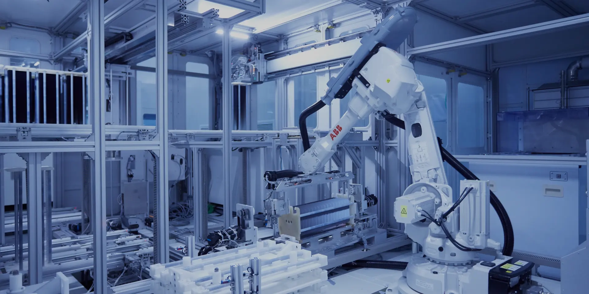
Streamlined Manufacturing Process
HJT technology requires only four core process steps, significantly fewer than the more than ten steps required for TOPCon and BC technologies. This results in higher yield, lower energy consumption, and improved process controllability.
HJT / C-HJT
4 Steps
TOPCon / BC
10+ Steps

Texturing & Cleaning

PECVD

PVD

Metallization Patterning
Low-Temperature Processing
All key production steps are completed at temperatures below 200°C, enabling the use of thinner silicon wafers while minimizing thermal damage and high-temperature diffusion, thereby substantially reducing silicon material consumption, overall energy costs, and the carbon footprint.
200°C
HJT
800°C
Other Solar Cells
Silver-free Solar Cell Manufacturing


Silver
155 kg CO₂/kg


Copper
3.97 kg CO₂/kg
- Silver-free C-HJT mass production cuts the carbon footprint of copper to just 2.56% of silver, significantly lowering overall emissions.
- Copper delivers electrical conductivity and mechanical strength comparable to silver, yet is 1,600 times more abundant and costs only one-tenth as much — making it an ideal, sustainable choice for the solar industry.
Dinto Solar HJT Solar Technology Roadmap


HJT Cell Tech
- Low-temperature gettering
- Multi-layer interfacial passivation films
- Double-sided microcrystalline silicon
- High-efficiency TCO thin films
- Rear-side polishing
- Edge passivation optimization
- 110 μm ultra-thin wafer mass production
- Ultra-narrow gridline printing
- High-precision copper gridlines
- HJT–perovskite tandem
HJT Module Tech
- Half-cut cells
- 1/3-cut cells
- Super Multi-Busbar (SMBB)
- Zero Busbar (0BB)
- Flexible interconnection
- Full-screen module design
- High-reflectivity triangular solder ribbons
- High-transmittance coated glass
- High-reliability encapsulation
- Lightweight & flexible encapsulation

C-HJT 1.0
1/3-cut + C-HJT 2.0
HJT–perovskite Tandem
≥ 23.18%
Module Efficiency
720W+
Module Power
2024
≥ 23.99%
Module Efficiency
745W+
Module Power
2025
≥ 24.47%
Module Efficiency
760W+
Module Power
2026
≥ 25.11%
Module Efficiency
780W+
Module Power
2027
≥ 25.75%
Module Efficiency
800W+
Module Power
2028
≥ 27.36%
Module Efficiency
850W+
Module Power
2029
≥ 32.20%
Module Efficiency
1000W+
Module Power
2030